
Industry
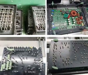
Process Differences and the Necessity of Tooling in Wave Soldering vs. Reflow Soldering
While Wave Soldering and Reflow Soldering are the twin pillars of PCB assembly, they require vastly different strategies to ensure quality.
Company
Official Notice: Product Price Adjustment
Due to the impact of global instability and the appreciation of the RMB, raw material costs in China have risen significantly.
Industry
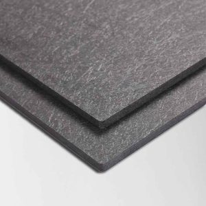
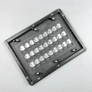
High-Performance PCB Solder Pallet & Fixture Material
Our PCB Solder Pallet Material is a game-changer for wave soldering—offering extreme thermal stability, ESD protection, and 20,000+ cycle durability.